- 您现在的位置:买卖IC网 > Sheet目录286 > 24C01C-I/ST (Microchip Technology)IC EEPROM 1KBIT 400KHZ 8TSSOP
�� �
�
�24C01C�
�6.0�
�6.1�
�WRITE� OPERATIONS�
�Byte� Write�
�After� the� receipt� of� each� word,� the� four� lower� order�
�Address� Pointer� bits� are� internally� incremented� by� one.�
�The� higher� order� four� bits� of� the� word� address� remains�
�constant.� If� the� master� should� transmit� more� than� 16�
�Following� the� Start� signal� from� the� master,� the� device�
�code� (4� bits),� the� Chip� Select� bits� (3� bits),� and� the� R/W�
�bit,� which� is� a� logic� low,� is� placed� onto� the� bus� by� the�
�master� transmitter.� The� device� will� acknowledge� this�
�control� byte� during� the� ninth� clock� pulse.� The� next� byte�
�transmitted� by� the� master� is� the� word� address� and� will�
�bytes� prior� to� generating� the� Stop� condition,� the�
�address� counter� will� roll� over� and� the� previously�
�received� data� will� be� overwritten.� As� with� the� byte� write�
�operation,� once� the� Stop� condition� is� received� an�
�internal� write� cycle� will� begin� (� Figure� 6-2� ).�
�be� written� into� the� Address� Pointer� of� the� 24C01C.�
�After� receiving� another� Acknowledge� signal� from� the�
�24C01C� the� master� device� will� transmit� the� data� word�
�to� be� written� into� the� addressed� memory� location.� The�
�24C01C� acknowledges� again� and� the� master� gener-�
�ates� a� Stop� condition.� This� initiates� the� internal� write�
�cycle,� and� during� this� time� the� 24C01C� will� not�
�generate� Acknowledge� signals� (� Figure� 6-1� ).�
�Note:�
�Page� write� operations� are� limited� to� writ-�
�ing� bytes� within� a� single� physical� page,�
�regardless� of� the� number� of� bytes� actu-�
�ally� being� written.� Physical� page� boundar-�
�ies� start� at� addresses� that� are� integer�
�multiples� of� the� page� buffer� size� (or� ‘page�
�size’)� and� end� at� addresses� that� are�
�integer� multiples� of� [page� size� –� 1].� If� a�
�6.2�
�Page� Write�
�Page� Write� command� attempts� to� write�
�across� a� physical� page� boundary,� the�
�The� write� control� byte,� word� address� and� the� first� data�
�byte� are� transmitted� to� the� 24C01C� in� the� same� way� as�
�in� a� byte� write.� But� instead� of� generating� a� Stop�
�condition,� the� master� transmits� up� to� 15� additional� data�
�bytes� to� the� 24C01C� which� are� temporarily� stored� in�
�the� on-chip� page� buffer� and� will� be� written� into� the�
�memory� after� the� master� has� transmitted� a� Stop�
�condition.�
�result� is� that� the� data� wraps� around� to� the�
�beginning� of� the� current� page� (overwriting�
�data� previously� stored� there),� instead� of�
�being� written� to� the� next� page� as� might� be�
�expected.� It� is� therefore� necessary� for� the�
�application� software� to� prevent� page� write�
�operations� that� would� attempt� to� cross� a�
�page� boundary.�
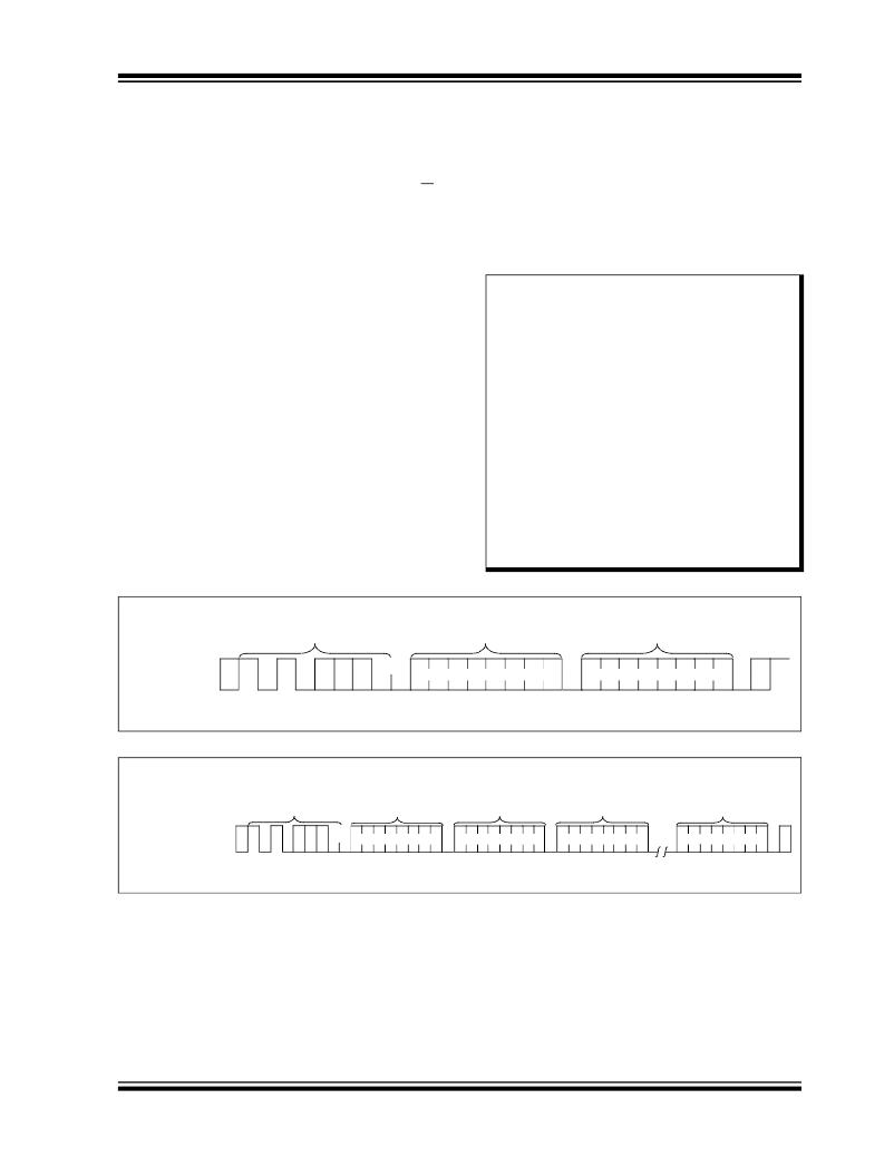
�FIGURE� 6-1:�
�BYTE� WRITE�
�Bus� Activity�
�Master�
�S�
�T�
�A�
�R�
�T�
�Control�
�Byte�
�Word�
�Address�
�Data�
�S�
�T�
�O�
�P�
�SDA� Line�
�S�
�P�
�Bus� Activity�
�FIGURE� 6-2:�
�PAGE� WRITE�
�A�
�C�
�K�
�A�
�C�
�K�
�A�
�C�
�K�
�Bus� Activity�
�Master�
�S�
�T�
�A�
�R�
�T�
�Control�
�Byte�
�Word�
�Address� (n)�
�Data� n�
�Data� n� +1�
�Data� n� +� 15�
�S�
�T�
�O�
�P�
�SDA� Line�
�S�
�P�
�Bus� Activity�
�A�
�C�
�K�
�A�
�C�
�K�
�A�
�C�
�K�
�A�
�C�
�K�
�A�
�C�
�K�
�?� 1997-2012� Microchip� Technology� Inc.�
�DS21201K-page� 9�
�发布紧急采购,3分钟左右您将得到回复。
相关PDF资料
24C02C-I/MC
IC EEPROM 2KBIT I2C 8DFN
24C08B-E/P
IC EEPROM 8KBIT 100KHZ 8DIP
24FC1026-I/P
IC EEPROM 1024KB 1MHZ 8-DIP
24FC128-I/MNY
IC EEPROM 128KBIT 1MHZ 8TDFN
24FC515T-I/SM
IC EEPROM 512KBIT 1MHZ 8SOIC
24FC64T-I/MF
IC EEPROM 64KBIT 1MHZ 8DFN
24LC014H-I/P
IC EEPROM 1KBIT 400KHZ 8DIP
24LC014T-E/OT
IC EEPROM 1KBIT 400KHZ SOT23-6
相关代理商/技术参数
24C01C-I/STG
功能描述:电可擦除可编程只读存储器 128x8 Lead Free Package
RoHS:否 制造商:Atmel 存储容量:2 Kbit 组织:256 B x 8 数据保留:100 yr 最大时钟频率:1000 KHz 最大工作电流:6 uA 工作电源电压:1.7 V to 5.5 V 最大工作温度:+ 85 C 安装风格:SMD/SMT 封装 / 箱体:SOIC-8
24C01C-IP
制造商:MICROCHIP 制造商全称:Microchip Technology 功能描述:1K 5.0V I 2 C ⑩ Serial EEPROM
24C01C-ISN
制造商:MICROCHIP 制造商全称:Microchip Technology 功能描述:1K 5.0V I 2 C ⑩ Serial EEPROM
24C01C-IST
制造商:MICROCHIP 制造商全称:Microchip Technology 功能描述:1K 5.0V I 2 C ⑩ Serial EEPROM
24C01CP
制造商:Microchip Technology Inc 功能描述:
24C01C-P
制造商:MICROCHIP 制造商全称:Microchip Technology 功能描述:1K 5.0V I 2 C ⑩ Serial EEPROM
24C01CSN
制造商:Microchip Technology Inc 功能描述:
24C01C-SN
制造商:MICROCHIP 制造商全称:Microchip Technology 功能描述:1K 5.0V I 2 C ⑩ Serial EEPROM